Microscopy & morphology services
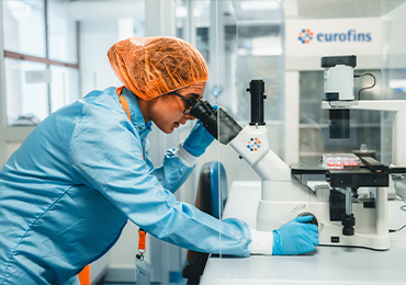
Expert imaging to understand materials and structures
You need total confidence in the smallest details of your device. From microelectronics to multilayered materials, the performance and safety of your product often depend on features invisible to the naked eye. Whether you're facing unexpected test failures, materials questions, or regulatory pressure, microscopic insight can bring clarity.
The Eurofins Medical Device Services network of laboratories uncovers that clarity. We offer comprehensive microscopy and morphology services to support materials characterization, defect analysis, and structural evaluation. With decades of combined experience and a diverse toolkit, our scientists apply the right techniques to solve complex surface and sub-surface problems. Such advanced microscopy allows medical device professionals to better visualize materials and observe designed structures and layers.
These techniques support investigations:
- Cross-sectional analysis of multilayered materials
- Identification of defects and particles
- Microelectronics and materials failures
- Reverse engineering
Our team works with clients to understand the molecular orientation and thickness, alongside the location of the defect and its structure. All the while meeting regulatory requirements, reducing development risks, and avoiding costly rework.