

- No Results
- Global
-
Australia

-
Austria

-
Azerbaijan

-
Brazil

-
Belgium

-
Canada

-
Chile

-
China

-
Costa Rica

-
Croatia

-
Czech Republic

-
Denmark

-
ESTONIA

-
Finland

-
France

-
Germany

-
Hong Kong

-
Hungary

-
India

-
Italy

-
Ireland

-
Japan

-
Korea

-
Latvia

-
Lithuania

-
Malaysia

-
Mexico

-
Morocco

-
Netherlands

-
New Zealand

-
Norway

-
Philippines

-
Poland

-
Portugal

-
Romania

-
Singapore
-
Slovakia

-
Slovenia

-
Spain

-
Sweden

-
Switzerland

-
Taiwan

-
Turkey

-
United Kingdom

-
UNITED ARAB EMIRATES

-
United States
-
Vietnam

Search >>
Microscopy & Morphology
Contact us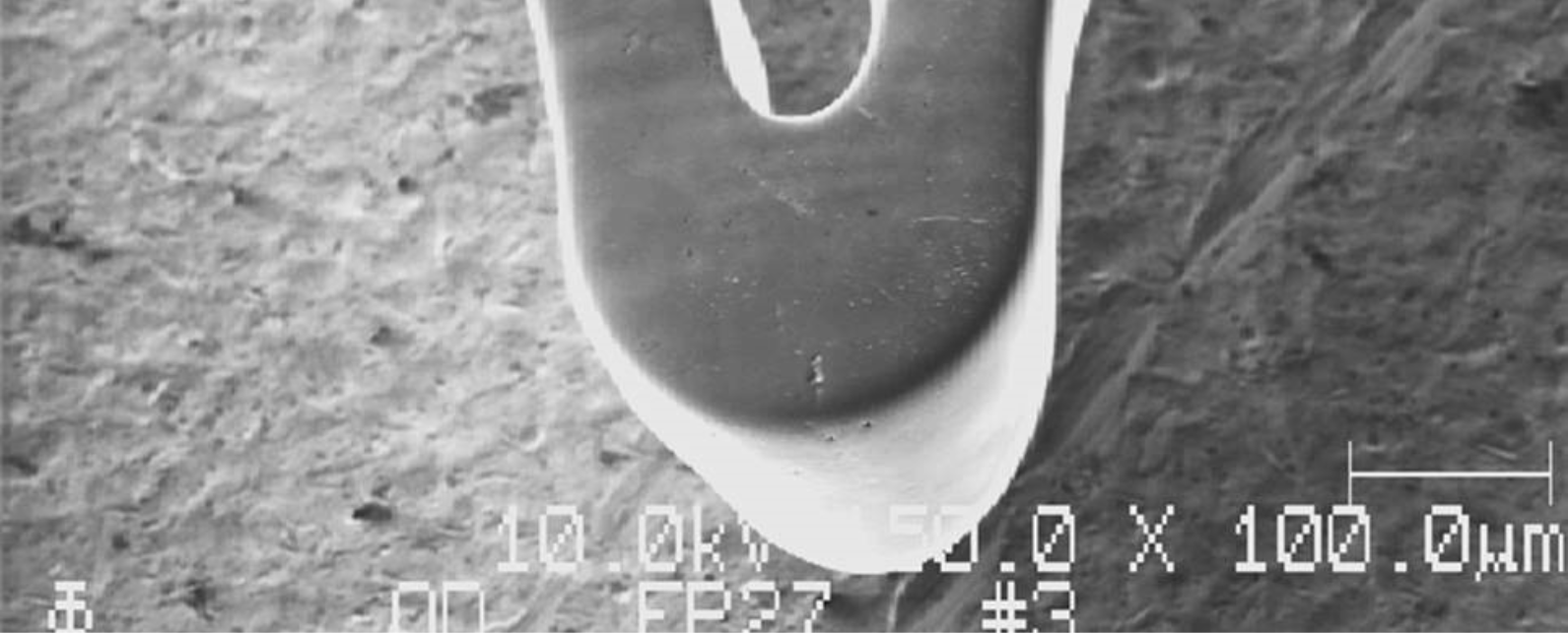
New technologies in medical devices and diagnostics are requiring smaller and smaller features to deliver unique treatment options. Advanced microscopy allows medical device professionals to better visualise materials and observe designed structures and layers. Advancements in microscopy have allowed for the further study of nanometer-scale features in conjunction with powerful sample preparation techniques.
We frequently encounter medical device professionals with the following questions about surface chemistry and properties:
- What is the molecular orientation?
- What is the thickness?
- What is the location of the defect and what is its structure?
Eurofins Medical Device Testing network of laboratories has years of experience in preparing and imaging a variety of materials with a diverse tool set. Typical techniques used include:
- SEM
- TEM/STEM
- FIB-SEM
- AFM
- Raman
- TOF-SIMS
- Auger
Choose Eurofins Medical Device Testing to help you with:
- Investigation of microelectronics and materials failures
- Reverse engineering
- Cross-sectional analysis of multilayered materials
- Analysis of defects and particles